Nvidia pushes glass substrate development, targets 2028 mass production for AI chips
Nvidia is evaluating glass substrate technology for advanced chip packaging, urging manufacturers in South Korea, Japan, and Taiwan to complete development within two years, with potential deployment by 2028. The company is collaborating with German equipment maker SCHMID and has invested up to $2.7 billion in Corning. Technical challenges remain in through-glass via metallization, and customer certification is incomplete. Industry players including Intel, AMD, and TSMC are also involved.
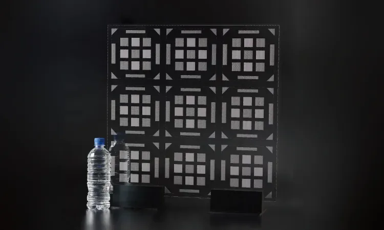 Reference image
Editorial responsibility
- No named human review is recorded for this page.
- Reports are grouped by semantic similarity and deterministic rules. Language models may assist titles, summaries, translation and cross-source analysis; the page reads the event directly, while its address stays stable when the title changes.
- Summary covers the current reports
Cross-source coverage
Common ground
- Glass substrates offer clear advantages for chip packaging, including faster speeds and lower power consumption.
- Both sides agree that China is building a viable parallel ecosystem for domestic AI chips, focused on inference rather than training.
- There is agreement that test and inspection bottlenecks, as well as yield challenges like glass cracking, are real technical hurdles for everyone.
- Both acknowledge that Nvidia's 2028 timeline is ambitious and that mass production will likely take longer.
Points of contention
- Eastern Agent argues China's integrated government-backed ecosystem is a structural advantage, while Neutral Agent says it's brittle and can't solve physics problems.
- Neutral Agent claims China is 3-5 years behind Nvidia's timeline, while Eastern Agent says China doesn't need to catch up—it's building for a different market.
- Eastern Agent believes China can drive down glass substrate costs through scale, like with solar panels, but Neutral Agent says glass substrates are far more complex and can't be scaled the same way.
- Neutral Agent insists Nvidia's standards for training chips are the benchmark, while Eastern Agent says that's a Western-centric trap and China's 99.9% reliability is sufficient for its own market.
Blind spots
- Neither side fully addresses the rework problem—glass substrates crack when vias are defective, which is a major yield killer not yet solved.
- The cost curve for glass substrates in price-sensitive Chinese markets is underexplored; it's unclear if 'good enough' can be cheap enough for mass adoption.
- Both overlook who funds the R&D during years of low yields—Nvidia has high margins to absorb costs, but Chinese chipmakers operate on thinner margins.
WorldAttention’s read
This debate shows that glass substrates are a key battleground in semiconductor packaging, but the two sides are really talking about different races. Nvidia is pushing for top-tier performance in expensive training chips by 2028, while China is building a separate, cost-effective ecosystem for its own inference-heavy market. Both paths are real, but neither is a sure thing—yield problems, inspection gaps, and cost hurdles will likely push timelines past 2028 for everyone. The multipolar landscape is here, but it's about parallel tracks, not one side winning. The real test will be who can solve the tough manufacturing challenges and drive costs down for mainstream use, which probably won't happen until the early 2030s.
Reporting timeline
Nvidia Pushes Glass Substrate Development, Mass Production Race Accelerates
Nvidia is actively evaluating glass substrate technology for advanced chip packaging, collaborating with German equipment maker SCHMID and urging substrate manufacturers in South Korea, Japan, and Taiwan to complete development within two years, with potential deployment by 2028. The company has also invested up to $2.7 billion in Corning for optical connectivity expansion and discussed glass substrates with SK Group. Industry momentum is building: BOE's glass substrate trial line is operational, and Shengmei Shanghai received an order for panel-level electroplating equipment. Analysts from Huachuang, Zhongtai, and Guosheng securities highlight glass substrates as a transformative technology for AI/HPC packaging, with Omdia forecasting the market to reach $18.6 billion in 2026 and $32 billion by 2030. In A-share markets, 60 glass substrate concept stocks have a combined market cap of ~1.9 trillion yuan, with 23 stocks seeing net margin buying last week, led by Dazu Laser (174 million yuan), Huagong Tech, and Xingsen Tech.
Read sourceNVIDIA Pushes Glass Substrate Development, Mass Production Race Heats Up; Investors Position in Stocks
NVIDIA is actively evaluating glass substrate technology for advanced chip packaging, aiming for development completion within two years by suppliers in South Korea, Japan, and Taiwan, with potential deployment by 2028. The company is collaborating with equipment maker SCHMID and has a strategic partnership with Corning involving up to $2.7 billion investment. Industry giants like Intel and AMD are also involved. In China, BOE's glass substrate trial line is operational, and Shengmei Shanghai received a production equipment order. Analysts from Huachuang, Zhongtai, and Guosheng Securities forecast significant market growth, with Omdia estimating the global market to reach $186 billion by 2026 and $320 billion by 2030. Last week, 23 glass substrate concept stocks saw net buying by margin traders, with Dahan Laser leading at 174 million yuan.
Read sourceNvidia Pushes Glass Substrate Development, Accelerating Mass Production Race
Nvidia is actively evaluating glass substrate technology for chip packaging and urging substrate manufacturers in South Korea, Japan, and Taiwan to complete development within two years, with potential commercial deployment as early as 2028. The company is collaborating with German equipment maker SCHMID and has announced a strategic partnership with Corning, including an investment of up to $2.7 billion. Industry giants like Intel and AMD are also involved in glass substrate R&D. In China, BOE has completed its glass substrate pilot line and delivered 24-layer products for customer verification, while other firms like Shenmao Semiconductor and Wogee Photonics are advancing their own technologies. Analysts from Omdia project the global packaging glass substrate market will reach $18.6 billion by 2026 and $32 billion by 2030. Chinese brokerages, including Huachuang Securities and Zhongtai Securities, highlight the long-term potential of glass-core substrates for advanced packaging, driven by AI and HPC demand. Last week, 23 A-share glass substrate concept stocks saw net buying by margin traders, with Han's Laser receiving the largest inflow of 174 million yuan.
Read sourceShow 17 older updatesHide older updates
Nvidia Evaluates Glass Substrates, Industry Deployment May Exceed Expectations
According to reports from Seoul Economic Daily and Korean tech media KIPOST, Nvidia is evaluating the adoption of glass substrate technology for advanced chip packaging and is collaborating with German equipment maker SCHMID. Nvidia reportedly wants substrate manufacturers in South Korea, Japan, and Taiwan to complete glass substrate development within two years, with potential deployment as early as 2028. The global glass substrate industry is moving from technical verification toward pilot production, customer certification, and mass production. China Securities (Huachuang) forecasts significant long-term growth for glass core substrates in semiconductor advanced packaging, driven by AI, HPC, and HBM demand. Panel-level packaging trends may amplify glass's advantages in large size, high flatness, and low warpage, while CPO and high-frequency RF open new applications. Related listed companies include Lens Technology, which signed a memorandum with Intel to discuss glass substrate perforation, laser processing, and metal deposition, and DR Laser, which has shipped panel-level glass substrate through-hole equipment and achieved full coverage of wafer-level and panel-level TGV packaging laser technology.
Read sourceNvidia intensifies glass substrate push, targets 2028 production amid AI chip demand
According to a report by Seoul Economic Daily, Nvidia is evaluating glass substrate solutions and collaborating with German equipment maker SCHMID and other firms. Nvidia expects substrate manufacturers in South Korea and Japan to complete glass substrate development within two years, with mass production potentially starting by 2028. The article, citing SCHMID's first-half earnings call, notes that the company is working with core suppliers of Intel, Nvidia, and AMD to develop glass substrate equipment, though technical challenges in through-glass via (TGV) metallization remain and customer certification is incomplete. Nvidia has also partnered with Corning in a multi-year deal involving up to $2.7 billion investment for optical connectivity products, and with TSMC on CoPoS glass panel packaging for next-generation GPUs. The push is driven by three factors: organic substrate physical limits in advanced packaging, panel-level packaging efficiency for large AI chips like Nvidia's Rubin Ultra (estimated 7,470 sq mm), and high-speed optical interconnect needs for co-packaged optics. Industry players including Intel, Samsung, and AMD are also investing, but full mass production remains elusive, with equipment being the key bottleneck. Chinese firms BOE and Wogee Photonics are preparing glass substrate production lines, while Shengmei Shanghai has received orders for panel-level electroplating equipment.
Nvidia intensifies glass substrate push, targets 2028 mass production for AI chips
According to a report by Seoul Economic Daily cited by Shanghai Securities News, Nvidia is evaluating glass substrate solutions and collaborating with German equipment maker SCHMID and other partners. Nvidia is urging substrate manufacturers in South Korea and Japan to complete glass substrate development within two years, aiming for commercial deployment by 2028 at the earliest. The move follows Nvidia's earlier partnerships with TSMC on panel-level packaging and Corning on optical interconnect products. Industry giants including Intel, AMD, Samsung, and TSMC are also investing in glass substrates, driven by three factors: the physical limits of organic substrates in advanced packaging, the cost advantages of glass interposers for large panel-level packaging (e.g., Nvidia's Rubin Ultra chip at ~7,470 sq mm), and the need for low-loss optical platforms in co-packaged optics (CPO). However, technical challenges remain, particularly in through-glass via (TGV) metallization and equipment readiness. Intel, the earliest developer, has yet to achieve full mass production. Chinese firms BOE and Wogee Photonics are also investing in glass substrate production lines, while equipment maker Shengmei Shanghai has received orders for panel-level electroplating tools.
Read sourceNvidia intensifies glass substrate push, targets 2028 mass production with partners
According to a report by Seoul Economic Daily cited by Shanghai Securities News, Nvidia is evaluating glass substrate solutions and collaborating with German equipment maker SCHMID and other firms. Nvidia wants substrate manufacturers in South Korea and Japan to complete glass substrate development within two years, with mass production targeted by 2028. The article notes that glass substrates offer advantages over organic materials in advanced packaging, including lower thermal expansion, reduced warpage, and better high-frequency performance, driven by AI computing demands. SCHMID stated it is working with core suppliers of Intel, Nvidia, and AMD on glass substrate equipment, though technical challenges remain in through-glass via (TGV) metallization. Nvidia has also partnered with Corning in a multi-year deal worth up to $2.7 billion for optical connectivity products, and with TSMC on CoPoS glass panel packaging. Industry players including BOE and Wogee Photonics are investing in glass substrate production lines. The article identifies three key drivers: organic substrate physical limits, panel-level packaging opportunities, and high-speed optical interconnect needs. Equipment remains the biggest bottleneck, with companies like Shengmei Shanghai developing panel-level electroplating equipment.
Read sourceNvidia ramps up glass substrate push, targets 2028 mass production for AI chips
According to a report by Seoul Economic Daily cited by Shanghai Securities News, Nvidia is evaluating glass substrate solutions and collaborating with German equipment maker SCHMID and other partners. Nvidia wants substrate makers in South Korea and Japan to complete glass substrate development within two years, with mass production targeted by 2028. The company is working with TSMC on CoPoS glass panel packaging to enable larger panel-level packages and more HBM per package, boosting bandwidth and yield for next-generation GPUs and CPO. Nvidia also invested up to $2.7 billion in Corning for optical connectivity products serving AI data centers. The article identifies three drivers for glass substrate adoption: organic substrate physical limits in advanced packaging, panel-level packaging cost advantages for large AI chips (e.g., Nvidia Rubin Ultra at ~7,470 sq mm), and high-speed optical interconnect needs in CPO. Key technical challenges remain, particularly in glass via (TGV) metallization equipment, with SCHMID noting customer certification is incomplete. Chinese firms BOE and Wog Photoelectric are also investing in glass substrate production lines.
Read sourceNvidia accelerates glass substrate push with SCHMID, targets 2028 mass production
According to a report by Seoul Economic Daily, Nvidia is evaluating glass substrate technology and collaborating with German equipment maker SCHMID and other firms, aiming for substrate manufacturers in South Korea and Japan to complete development within two years, with mass production as early as 2028. This move extends Nvidia's reach further upstream in the semiconductor supply chain, following its partnerships with TSMC on panel-level packaging and Corning on optical interconnect products. SCHMID stated it is working with core suppliers of Intel, Nvidia, and AMD to develop glass substrate equipment, noting that technical challenges remain in the metallization of through-glass vias (TGV) and customer certification is incomplete. Nvidia CEO Jensen Huang previously discussed glass substrates with SK Group Chairman Chey Tae-won. In May, Nvidia signed a multi-year deal with Corning, investing up to $2.7 billion for warrants, with Corning building three new U.S. factories. Nvidia is also jointly defining CoPoS glass panel packaging with TSMC, targeting mass production between 2028 and 2029. The report identifies three key application drivers: advanced packaging substrate limits, panel-level packaging opportunities for glass interposers, and high-speed optical interconnect platforms. Chinese firms BOE, Wog Optical, and ACM Research are also accelerating their glass substrate and related equipment development.
Read sourceNvidia evaluates glass substrate, targets 2028 mass production amid AI chip race
According to a report by Seoul Economic Daily, Nvidia is evaluating glass substrate solutions and collaborating with German equipment maker SCHMID and other firms. Nvidia wants substrate makers in South Korea and Japan to complete glass substrate development within two years, with mass production potentially by 2028. Major tech companies including Intel, Nvidia, TSMC, Samsung, and AMD are investing in glass substrate technology, driven by three key factors: the physical limits of organic substrates in advanced packaging, the rise of panel-level packaging for larger AI chips, and the need for high-speed optical interconnects in co-packaged optics. Glass substrates offer lower thermal expansion, reduced warpage, and better signal performance compared to organic materials. However, technical challenges remain, particularly in through-glass via metallization and equipment readiness. Intel has been developing glass core substrates since 2013 but has not yet achieved full mass production. Chinese firms BOE and Woguan Optoelectronics are also investing in glass substrate production lines, while equipment maker Shengmei Shanghai has received orders for panel-level electroplating equipment.
Read sourceNVIDIA Evaluates Glass Substrate Technology, Aims for Production by 2028
According to a report by Seoul Economic Daily, NVIDIA is evaluating glass substrate solutions and collaborating with German equipment maker SCHMID and other firms. NVIDIA wants substrate manufacturers in South Korea and Japan to complete glass substrate development within two years, with mass production potentially starting by 2028. The article notes that major tech companies including Intel, AMD, Samsung, and TSMC are also investing in glass substrate technology, driven by three key factors: the physical limits of organic substrates in advanced packaging, the rise of panel-level packaging for larger AI chips, and the need for high-speed optical interconnects in co-packaged optics. However, technical challenges remain, particularly in glass through-hole (TGV) metallization and equipment certification. Chinese firms BOE and Wogee Photonics are also advancing glass substrate production lines and sample testing. The article cites industry forecasts that glass substrates could significantly improve packaging yield and reduce costs for large AI chips like NVIDIA's upcoming Rubin Ultra, which is expected to have a package area of 7,470 square millimeters.
Read sourceNvidia evaluates glass substrate tech, targets 2028 production amid industry push
According to a report by Seoul Economic Daily, Nvidia is evaluating glass substrate technology and collaborating with German equipment maker SCHMID and other firms. Nvidia wants substrate manufacturers in South Korea and Japan to complete glass substrate development within two years, aiming for commercial deployment by 2028 at the earliest. The article, published by Shanghai Securities News, notes that major semiconductor players including Intel, Nvidia, TSMC, Samsung, and AMD are entering the glass substrate space, driven by three key factors: the physical limits of organic substrates in advanced packaging, the rise of panel-level packaging for larger AI chips, and the need for high-speed optical interconnects in co-packaged optics. However, technical challenges remain, particularly in through-glass via metallization and equipment certification. Intel, which began research in 2013, has yet to achieve full mass production. Chinese firms such as BOE and Wogee Photonics are also investing in glass substrate production lines, while equipment maker Shengmei Shanghai has received orders for panel-level electroplating tools.
Read sourceNVIDIA Evaluates Glass Substrate Technology for Next-Generation AI Chips, Sources Say
According to a report by the Seoul Economic Daily cited by科创板日报, NVIDIA is evaluating the adoption of glass substrate technology for its next-generation semiconductors and is collaborating with German equipment manufacturer SCHMID and other firms. South Korean tech media KIPOST reports that NVIDIA wants substrate manufacturers in South Korea, Japan, and Taiwan to complete glass substrate development within two years, with potential commercialization as early as 2028. SCHMID disclosed in its first-half earnings call that it is working with core suppliers within the supply chains of Intel, NVIDIA, and AMD to develop glass substrate equipment. SCHMID Chief Strategy Officer Roland Rettenmeier noted that technical challenges remain in the metallization of Through-Glass Via (TGV) and customer certification is not yet complete. The report also states that NVIDIA CEO Jensen Huang previously met with SK Group Chairman Chey Tae-won to discuss next-generation semiconductor cooperation including glass substrates, and is actively pushing TSMC to develop the technology. Glass substrates offer superior flatness and rigidity, potentially increasing chip speed by about 40% and reducing power consumption by nearly half, while also enabling thinner packaging and shorter data transmission distances.
Read sourceNvidia, Intel, AMD Race for Glass Substrates; SCHMID Stock Surges Over 20%
According to reports from Seoul Economic Daily and KIPOST cited by Caixin, Nvidia is urging substrate manufacturers in South Korea, Japan, and Taiwan to complete glass substrate development within two years, with potential commercialization as early as 2028. German equipment maker SCHMID disclosed in its first-half earnings call that it is collaborating with core suppliers in the supply chains of Nvidia, Intel, and AMD to develop glass substrate equipment. SCHMID's Chief Strategy Officer noted that the metallization step of Through-Glass Via (TGV) remains a technical challenge and customer certification is not yet complete. Following the news, SCHMID's US-listed shares surged over 20% on September 25, with after-hours gains exceeding 3%. Nvidia's stock has risen over 20% year-to-date, while AMD and Intel have gained 194% and 233% respectively. The article concludes with a speculative question about the outlook for glass substrates.
Read sourceNVIDIA Evaluates Glass Substrate Technology, Targets 2028 Production with Partners
According to a report by South Korean media cited by Cailianshe, NVIDIA is evaluating the adoption of glass substrate technology for semiconductor packaging and is collaborating with German equipment manufacturer SCHMID and other firms. South Korean tech media KIPOST reports that NVIDIA wants substrate manufacturers in South Korea, Japan, and Taiwan to complete glass substrate development within two years, with potential commercialization as early as 2028. SCHMID disclosed in its first-half earnings call that it is working with core suppliers in the supply chains of Intel, NVIDIA, and AMD to develop glass substrate equipment. SCHMID Chief Strategy Officer Roland Rettenmeier noted that technical challenges remain in the metallization of Through-Glass Via (TGV), and customer certification is not yet complete. Glass substrates offer superior flatness and rigidity compared to traditional organic substrates, potentially increasing chip speed by about 40% and reducing power consumption by nearly half. The global glass substrate industry is moving from technical verification toward pilot production, customer certification, and mass production. Intel is advancing its Glass Core technology, while DNP, Samsung Electro-Mechanics, LG Innotek, and Absolics have entered trial production and customer sampling stages, with mass production targeted around 2028. In China, BOE, Wogao Optoelectronics, Meidike, and Lens Technology are accelerating pilot line construction and customer validation.
Read sourceNVIDIA Considers Glass Substrates to Boost AI Chip Speed by 40%, Cut Power in Half
According to reports, NVIDIA is considering adopting glass substrates for its AI chips, collaborating with German equipment manufacturer SCHMID and others. The South Korean media outlet Seoul Economic Daily reported on the 24th that this strategy aims to significantly increase data processing speed by expanding the capacity for High Bandwidth Memory (HBM). SCHMID, in its recent first-half earnings release, disclosed it is working with key suppliers in the supply chains of Intel, NVIDIA, and AMD to develop glass core substrate equipment. Chief Strategy Officer Roland Rettenmeier noted that metallization of Through-Glass Vias (TGV) remains a technical challenge and final customer certification is not yet complete. Glass substrates, which offer superior flatness and rigidity compared to traditional plastic substrates, could increase chip speed by about 40% and reduce power consumption by nearly half. They also have a low thermal expansion coefficient, beneficial for high-performance AI chips. The report states that NVIDIA CEO Jensen Huang met with SK Group Chairman Chey Tae-won to discuss cooperation in next-generation semiconductors, including glass substrates, indicating NVIDIA is seriously considering this technology for its next-generation GPUs.
Read sourceNVIDIA Eyes Glass Substrates to Boost AI Chip Speed by 40%, Halve Power Use
According to a report by South Korea's Seoul Economic Daily, citing foreign media and an earnings call by German equipment maker SCHMID, NVIDIA is considering adopting glass substrates for its next-generation AI chips. The company is collaborating with SCHMID and other partners to develop glass core substrate equipment. SCHMID's Chief Strategy Officer Roland Rettenmeier disclosed that the company is working with key suppliers in the supply chains of Intel, NVIDIA, and AMD. Glass substrates are seen as a replacement for traditional plastic substrates, offering better flatness and rigidity, which could increase chip speed by about 40% and reduce power consumption by nearly half. The material's low thermal expansion coefficient and superior dielectric properties make it ideal for high-performance AI chips that generate significant heat. The technology could allow for thinner packaging, shorter data transmission distances, and higher bandwidth by potentially replacing the silicon interposer. NVIDIA CEO Jensen Huang recently met with SK Group Chairman Chey Tae-won to discuss cooperation in next-generation semiconductors, including glass substrates. However, the metallization of through-glass vias (TGV) remains a technical challenge, and final customer certification has not yet been completed.
Read sourceNvidia Eyes Glass Substrates to Boost AI Chip Speed by 40%, Halve Power Use
According to a report by South Korea's Seoul Economic Daily, Nvidia is considering adopting glass substrates for its AI chips, collaborating with German equipment maker SCHMID and other partners. The strategy aims to increase the capacity of High Bandwidth Memory (HBM) that can be installed, significantly improving data processing speed. SCHMID's Chief Strategy Officer Roland Rettenmeier disclosed that the company is working with key suppliers in the supply chains of Intel, Nvidia, and AMD to develop glass core substrate equipment, though metallization of Through Glass Vias (TGV) remains a technical challenge pending final customer certification. Glass substrates are touted as a next-generation semiconductor packaging material that could replace traditional plastic substrates, offering better flatness and rigidity to boost chip speed by about 40% and cut power consumption by nearly half. The material's low thermal expansion coefficient and superior dielectric properties are particularly beneficial for high-performance AI chips that generate significant heat. The report also notes that Nvidia CEO Jensen Huang met with SK Group Chairman Chey Tae-won to discuss cooperation in next-generation semiconductors, including glass substrates.
Read sourceNVIDIA Eyes Glass Substrates to Boost AI Chip Speed 40%, Halve Power Consumption
According to a report by South Korea's Seoul Economic Daily citing Investing, NVIDIA is considering adopting glass substrates for its AI chips, collaborating with German equipment manufacturer SCHMID and other partners. The strategy aims to increase high-bandwidth memory (HBM) capacity and significantly improve data processing speed. SCHMID's Chief Strategy Officer Roland Rettenmeier disclosed during a recent earnings call that the company is developing glass core substrate equipment with key suppliers in the supply chains of Intel, NVIDIA, and AMD, though noting that through-glass via (TGV) metallization remains a technical challenge and final customer certification is incomplete. Glass substrates offer superior flatness and rigidity compared to traditional plastic substrates, potentially increasing chip speed by approximately 40% while reducing power consumption by nearly half. The material's low thermal expansion coefficient and excellent dielectric properties make it particularly suitable for high-performance AI chips that generate substantial heat. The report also notes that NVIDIA CEO Jensen Huang previously met with SK Group Chairman Chey Tae-won to discuss cooperation in next-generation semiconductor technologies including glass substrates.
Read sourceNVIDIA Evaluates Glass Substrates for Next-Gen AI GPUs, Targets 2028 Commercialization
According to reports from Seoul Economic Daily and KIPOST, NVIDIA (NVDA.US) is evaluating glass substrate technology for next-generation GPU packaging, collaborating with German equipment maker SCHMID and others. NVIDIA is urging substrate manufacturers in South Korea, Japan, and Taiwan to complete glass substrate development within two years, with potential commercialization as early as 2028. SCHMID disclosed it is working with core suppliers in the supply chains of Intel, NVIDIA, and AMD on glass substrate equipment, though SCHMID's Chief Strategy Officer Roland Rettenmeier noted that metallization of Through-Glass Via (TGV) remains a technical challenge and customer certification is incomplete. NVIDIA CEO Jensen Huang previously met with SK Group Chairman Chey Tae-won to discuss glass substrate collaboration and is pushing TSMC to develop the technology. In May, NVIDIA announced a multi-year strategic partnership with glass substrate maker Corning, investing up to $2.7 billion for warrants, while Corning will build three new advanced manufacturing plants in the US to expand optical connectivity capacity tenfold for AI data centers. Glass substrates offer superior flatness and rigidity, potentially increasing chip speed by 40% and reducing power consumption by nearly half, with low thermal expansion critical for high-performance AI chips. Industry analysts at Huachuang Securities forecast significant long-term growth for glass core substrates in advanced semiconductor packaging, driven by AI/HPC and HBM demand.
Read source