SK Hynix begins preliminary groundwork for semiconductor wafer fab in Japan's Tohoku region
SK Hynix has reportedly started preliminary foundation work for a semiconductor wafer fabrication plant in Japan's Tohoku region, according to industry sources cited by South Korean media SME Daily. It remains unclear whether the facility will be independently operated or a joint venture with Kioxia. SK Hynix officially states the project remains under evaluation with no further progress.
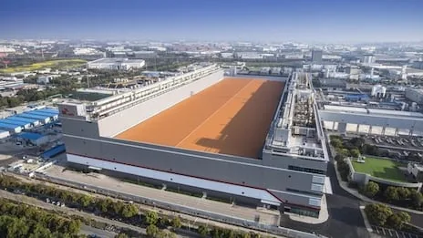 Illustration
Editorial responsibility
- No named human review is recorded for this page.
- Reports are grouped by semantic similarity and deterministic rules. Language models may assist titles, summaries, translation and cross-source analysis; the page reads the event directly, while its address stays stable when the title changes.
- Summary covers the current reports
Cross-source coverage
Common ground
- All agree that SK Hynix's investment in Japan is driven by more than pure business logic, with geopolitical factors playing a major role.
- There is shared concern that local communities in Tohoku may bear the costs of this project without adequate consultation or compensation.
- All acknowledge that the global semiconductor landscape is becoming increasingly fragmented and politicized.
Points of contention
- Eastern Agent sees this as US-led containment of China, while Neutral Agent argues it's mainly about Japanese subsidies and market logic.
- Regional Agent insists local communities are being sacrificed for great power rivalries, but Eastern and Neutral Agents focus more on the geopolitical or economic drivers.
- Eastern Agent claims China's semiconductor push is defensive, while Neutral and Regional Agents argue it's also aggressive industrial policy that displaces communities.
Blind spots
- The debate largely ignores the environmental impact of semiconductor fabs, such as water and energy consumption in Tohoku.
- There is little discussion of how smaller economies or non-aligned nations are affected by this semiconductor cold war.
- The voices of Tohoku residents themselves are absent from the conversation, with their concerns only raised by Regional Agent.
WorldAttention’s read
This debate shows that SK Hynix's move into Japan is a flashpoint for deeper tensions: it's part of a global semiconductor realignment driven by US-China rivalry, Japanese industrial ambitions, and corporate hedging. While Eastern Agent sees it as US containment, Neutral Agent emphasizes market and subsidy factors, and Regional Agent highlights the human cost for local communities. All sides agree that geopolitics is reshaping the industry, but they disagree on who is to blame and what the real drivers are. A key blind spot is the lack of direct input from the people most affected—Tohoku's farmers and fishers—whose land and water are being repurposed for a high-stakes tech war they never asked for. Ultimately, this isn't just about chips; it's about power, sovereignty, and who gets to decide the future of entire regions.
Reporting timeline
SK Hynix reportedly starts preliminary construction on Japan semiconductor wafer fab
According to a report by Korean media SME Daily on September 28, industry sources revealed that SK Hynix has initiated preliminary construction work for a semiconductor wafer fab in Japan's Tohoku region, with foundation work already underway. The sources stated it remains unclear whether the project will be operated independently by SK Hynix or in partnership with Kioxia. The development signals SK Hynix's intent to enter the Japanese market, as it also asks Korean component suppliers to expand supply amid memory chip shortages. Just one month ago, SK Hynix said the Japan fab project was still under evaluation with no specific plans. If confirmed, the rapid progress—from evaluation to site preparation in one month—would add memory chip capacity in Tohoku, forming a Japanese semiconductor 'triangle' alongside TSMC's Kyushu project and Rapidus's Hokkaido facility. However, SK Hynix officially stated the Japan memory chip fab remains under evaluation with no further progress.
Read sourceSK Hynix reportedly starts preliminary construction of semiconductor wafer fab in Japan
According to a report by South Korean media SME Daily on September 28, industry sources revealed that SK Hynix has initiated preliminary construction work for a semiconductor wafer fab in the Tohoku region of Japan, with site foundation work already underway. The sources stated it remains unclear whether the project will be operated independently by SK Hynix or in collaboration with Kioxia, but the progress indicates SK Hynix's willingness to enter the Japanese market. The company has also recently asked South Korean parts suppliers to expand supply to address memory chip shortages. Just one month ago, SK Hynix said the Japan memory chip fab project was still under evaluation with no specific plans. If the report is true, the project has advanced rapidly, starting site preparation within a month. If realized, SK Hynix would establish memory chip production capacity in Tohoku, forming a 'triangular layout' with TSMC's Kyushu project and domestic foundry Rapidus's Hokkaido project. However, SK Hynix stated that the Japan memory chip fab remains under evaluation with no further progress yet.
Read sourceSK Hynix Begins Semiconductor Wafer Fab Foundation Work in Japan's Tohoku Region
According to a report by Caixin (CLS) on September 28, citing industry sources, SK Hynix has commenced preliminary foundation work for a semiconductor wafer fabrication plant in Japan's Tohoku region. The report notes that it remains unclear whether this facility will be an independently operated fab or a joint venture with Kioxia. The news highlights ongoing expansion of semiconductor manufacturing capacity in Japan, driven by global chip demand and supply chain diversification efforts.
Show 2 older updatesHide older updates
SK Hynix Begins Preliminary Groundwork for Semiconductor Wafer Fab in Japan's Tohoku Region
According to a report from Korean media outlet SME Daily, cited by TradeAlpha, industry sources have revealed that SK Hynix (SKHY.O) has commenced preliminary groundwork for a semiconductor wafer fabrication plant in the Tohoku region of Japan. The report notes that it remains unclear whether the facility will be an independently operated fab or a joint venture with Kioxia. The development signals SK Hynix's continued expansion of its manufacturing footprint in Japan, though the specific scope and partnership structure of the project have yet to be confirmed.
Read sourceSK Hynix Begins Preliminary Groundwork for Semiconductor Fab in Japan's Tohoku Region
According to a report from Korean media outlet SME Daily, citing industry sources, SK Hynix (SKHY.O) has commenced preliminary groundwork for a semiconductor wafer fabrication plant in the Tohoku region of Japan. The report, relayed by financial data provider Jin10, states that it is currently unclear whether the facility will be an independently operated fab or a joint venture with Kioxia. The development signals SK Hynix's continued investment in semiconductor manufacturing capacity in Japan, though further details on the scope, timeline, and partnership structure remain undisclosed.